Get a quote

HDI PCB

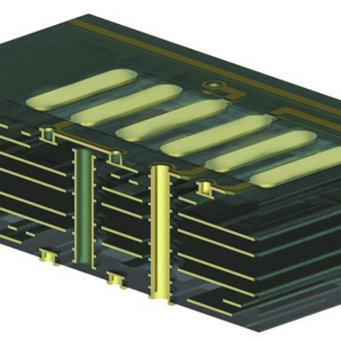
High-dense-interconnect PCB boards have a higher wiring density per unit area than typical PCBs. With changing technology, printed circuit board technology has evolved to meet the demand for smaller and faster products. HDIs have denser wiring, resulting in lighter, more compact PCBs. Instead of using several PCBs in a device, one HDI board can replace all the preceding boards.

Why choose HDI printed circuit boards?

The ability to “do more with less” is the primary advantage of HDI printed circuit boards with technology constantly seeking greater precision. HDI PCBs enable the deployment of many transistors for improved electronics performance while lowering power consumption. Because of the shorter distance connections and lower power requirements, signal integrity is also enhanced.

Modern designs often require highly advanced BGA with very fine pitch, which is impossible to fanout without HDI technology.

Microvias are also more dependable than through holes because they have a smaller aspect ratio; they are more reliable than typical through holes, allowing HDIs to achieve remarkable performance with superior materials and parts.

Where are HDI PCBs used?

HDI PCB board is usually found in complex electronic devices that demand excellent performance while conserving space. Applications include mobile /cellular phones, touch-screen devices, laptops, digital cameras, 4/5G network communications, and military applications such as avionics and smart munitions.

Automotive and aerospace industries, where lower weight can mean more efficient operation, have been utilizing HDI PCBs at an increasing rate. For example, today’s cars have around 50 microprocessors on board that play a role in engine controls, diagnostics, safety features, and other conveniences.

The high-density technology promotes improved performance and smaller, more cost-effective medical devices, potentially improving the accuracy of monitoring and medical testing.

HDI printed circuit boards play a significant role in industrial automation and IoT, as it is becoming more common in manufacturing, warehousing, and other industrial settings. Businesses use electronic tools to keep track of inventory and monitor equipment performance, collect usage data, and connect to the internet to communicate with other smart devices, as well as to relay information to management and help optimize operations.

Capabilities

Feature

Capability

Number of Layers

4-30 layers

Quality Grade

IPC 6016 Class 2, IPC 6016 Class 3

Material

Tg 150°C FR4, Tg 170°C FR4, Tg >170°C FR4, Special material

Thickness

0.4 - 6.0 mm

Min Track / Spacing

2-8 mil

Min Hole Size

0.15 mm - 0.3 mm

Solder Mask

Green, Red, Yellow, Blue, White, Black, Purple, Matte Black, Matte Green

Silkscreen

White, Black, Yellow, Blue

Surface Finish

Immersion gold, OSP, Hard Gold, Immersion Silver

Finished Copper

0.5-13 oz

Manufacturing time

5-10 days

Transport time

1-3 days

All you need to know about HDI PCB

HDI

HDI is a shortening of “High Dense interconnect” and are meant to describe a design solution that can make circuit hardware more compact. More or less, a direct reference to a PCB with blind and/or hidden via holes.

More than 2 layers, up to as many as the current PCB factory can handle in his multilayer process.

Thickness is not limited when designing a HDI PCB. However its important to consider the distance between layers that shall be connected, since size of via hole stands in direct relation to its depth.

A blind via is a hole that are not fully drilled trough the PCB. Its drilled from a outer layer to a innerlayer. The very point is that it stops at a certain innerlayer and not occupy area on other innerlayers or on the other side of the PCB.

A burried via, is a via hole that are drilled between innerlayers only, and will not occupy area on any outerlayer. Often also called hidden via hole.

A hidden via, is a via hole that are drilled between innerlayers only, and will not occupy area on any outerlayer. Often also called buried via hole.

IPC revised the definition of a microvia in 2013 to a hole with depth to diameter aspect ratio of 1:1 or less, and the hole depth not to exceed 250um. Before revision, “microvia” was any hole less than or equal to 0.15 mm in diameter, that often made it easy to misunderstand.

Its several blind vias located on the same place to create a deeper connection that should be possible with a single blind via. The single holes in a stacked via have to be cap-plated with copper to make electrical connection to the hole above.

Explore our other products

Standard PCB

Our definition of “Standard PCB” is a rigid glass-fibre board with one or more layers.

Flexible PCB

Flexible printed circuit boards get the name from the ability to be bent in a working application.

Rigid-Flex PCB

RIGID-FLEX PCB excels in overcoming space and weight constraints due to spatial degrees of freedom.

Metal Core PCB

A metal core printed circuit board uses metal as its base material to spread heat accumulated due to some electronic components operating on the board throughout the board.

High-Frequency PCB

High-frequency PCBs are often needed while developing high-frequency products, such as satellite systems, radio frequency, microwave, mobile telephone base stations, etc.

Solder Paste Stencils

Customized high-precision laser-cut solder paste stencils are used by the subcontractor assembly company to apply solder paste with high accuracy to all places that shall be soldered.

Prototypes & Pilot Runs

PCB prototyping can be the most important step during electronic development.

Learn more how we ensure quality of our products.

Learn more

Capabilities

Feature Capability
Number of Layers 4-30 layers
Quality Grade IPC 6016 Class 2, IPC 6016 Class 3
Material Tg 150°C FR4, Tg 170°C FR4, Tg >170°C FR4, Special material
Thickness 0.4 - 6.0 mm
Min Track / Spacing 2-8 mil
Min Hole Size 0.15 mm - 0.3 mm
Solder Mask Green, Red, Yellow, Blue, White, Black, Purple, Matte Black, Matte Green
Silkscreen White, Black, Yellow, Blue
Surface Finish Immersion gold, OSP, Hard Gold, Immersion Silver
Finished Copper 0.5-13oz
Manufacturing time 5-10 days
Transport time 1-3 days

Contact sales

Let’s get this conversation started. Tell us a bit about yourself, and your needs. We will get back to you within few hours.

Get a quotation

    We will get back to you within few hours