Let’s get this conversation started. Tell us a bit about yourself, and your needs. We will get back to you within few hours.
Design guidelines
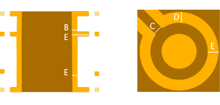
Pattern classes represent the PCB complexity. Higher class, may result in higher production cost.
Guide
Pattern classes
M5
M6
M7
M8
M9
Annular ring, hole -pattern outer layer pad
>200
>165
>140
>125
>100
A
Annularring, hole -pattern inner layer pad
>150
>140
>112
>100
>75
B
Trackwidth -inner -outerlayer
>200
>150
>125
>100
>75
C
Insulation inner -outerlayer
>200
>150
>125
>100
>75
D
Insulation -innerlayer to different net
>355
>300
>250
>200
>190
E
Clearance soldermask -soldersurface
>100
>90
>75
>50
>50
F
Pattern classes, reference views: